
What is a Diode?
Di+Ode is a semiconductor device with two terminals allowing the flow of current in one direction only, diodes are made up of Silicon, Germanium & GaAs. The perfect diode would be a perfect conductor in one direction (forward bias) and a perfect insulator in the other direction (reverse bias). In many situations, using the ideal diode approximation is acceptable.
In electronics, a diode is a two-terminal electronic component that conducts primarily in one direction. A diode has low, ideally zero, resistance to the flow of current in one direction, and high ideally infinite resistance in the other direction. Diode was invented in 1904 by John Ambrose Fleming. First diode was constructed with 2 electrodes in the form of a vacuum tube. In 1906, Lee Dee Forest added a 3rd electrode called a control grid and the triode, which is used as amplifier, switch. The application of triode created a new era in broadcasting with the invention of the crystal radio sensor by Pickard in 1912 which is commonly used in DC power supply units as a rectifiers and voltage regulators, clipper, clamper circuit. Diode now comes in different shape and sizes, below is shown a symbol and shape of a diode.
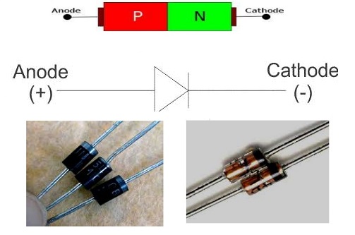
Diodes are made from a combination of 2 extrinsic semiconductors, P-type ad N-type material. The joint between the P-type and N-type material is called PN junction which have 2 terminals ( anode and cathode). Diodes are produced from the silicon wafer.
Semiconductor Diode Theory
Semiconductor diode theory is at the very center of much of today’s electronics industry. In fact semiconductor technology is present in almost every area of modern day technology and as such semiconductor theory is a very important element of electronics. A Semiconductor diode is a simple electrical device that allows the flow of current only in one direction. So it can be said to act somewhat like a switch. It is derived from “di-ode ” which means a device having two electrodes. In its basic form a semiconductor diode is formed by making P-N Junction which is one of the fundamental structures within semiconductor technology.
P-N Junction Usage
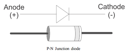
P-N Junction is the fundamental building block of semiconductor diodes and transistors and a number of other electronic components. It is formed by joining a P-Type (intrinsic semiconductor doped with a trivalent impurity) and N-Type semiconductor (intrinsic semiconductor doped with a pentavalent impurity) together with a special fabrication technique such that a P-N Junction is formed. Hence it is a device with two elements, the P-Type forms anode and has an excess of holes whereas, the N-Type forms the cathode and has an excess of electrons. These terminals are brought out to make the external connections. The symbol of a P-N Junction diode is shown below, the arrow head points in the direction of conventional current flow.
Application of Diodes in Daily Use
- Rectifying power supply circuit
- signal sensor in radar
- Voltage regulator in power supply circuit.
- Voltage clipper in power supply circuit
- Indicator light in electronic circuit
- Oscillator circuit in an oscilloscope
- Variable capacitor in a tune circuit
- Light sensor in a remote control unit
- Focused single colour light source in compact disc player
A semiconductor diode, the most common type today, is a crystalline piece of semiconductor material with a p–n junction connected to two electrical terminals. A vacuum tube diode has two electrodes, a plate (anode) and a heated cathode. Semiconductor diodes were the first semiconductor electronic devices. The discovery of crystals’ rectifying abilities was made by German physicist Ferdinand Braun in 1874. The first semiconductor diodes, called cat’s whisker diodes, developed around 1906, were made of mineral crystals such as galena. Today, most diodes are made of silicon, but other semiconductors such as selenium or germanium are sometimes used.
Zener Diode Introduction & Construction
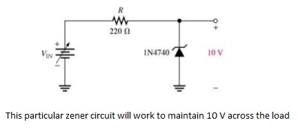
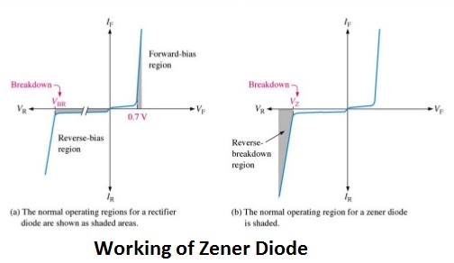
The zener diode is a silicon PN Junction device that differs from rectifier diodes because it is designed for operation in the reverse-breakdown region. The breakdown voltage of a zener diode is set by carefully controlling the level during manufacture. The basic function of zener diode is to maintain a specific voltage across it’s terminals within given limits of line or load change. Typically it is used for providing a stable reference voltage for use in power supplies and other equipment.
Construction of Zener Diodes
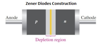
Zener diodes are designed to operate in reverse breakdown. Two types of reverse breakdown in a zener diode are avalanche and zener. The avalanche break down occurs in both rectifier and zener diodes at a sufficiently high reverse voltage. Zener breakdown occurs in a zener diode at low reverse voltages. A zener diode is heavily doped to reduced the breakdown voltage. This causes a very thin depletion region. The zener diodes breakdown characteristics are determined by the doping process Zeners are commercially available with voltage breakdowns of 1.8 V to 200 V.
Working of Zener Diodes
A zener diode is much like a normal diode. The exception being is that it is placed in the circuit in reverse bias and operates in reverse breakdown. This typical characteristic curve illustrates the operating range for a zener diode. Note that it’s forward characteristics are just like a normal diode.
Schottky Diode Introduction Working and Applications
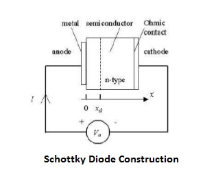
Schottky diode is one type of electronic component, which is also known as a barrier diode. It is widely used in different applications like a mixer, in radio frequency applications, and as a rectifier in power applications. It’s a low voltage diode in which N-type semiconductor acts as a cathode and the metal side acts as the anode of the diode. Schottky diode is also known as a hot carrier diode. It’s a low voltage diode. In a Schottky diode the voltage drop normally ranges between 0.15 and 0.45volts, this lower voltage drop provides higher switching speed and better system efficiency. In Schottky diode, a semiconductor–metal junction is formed between a semiconductor and a metal.
Schottky Diode Construction
Schottky Diode is a unilateral junction. A metal semiconductor junction is formed at one end and another metal semiconductor contact is formed at the other end. It is an ideal Ohmic bidirectional contact with no potential existing between the metal and the semiconductor. Schottky diode is a function of temperature dropping. It decreases and increasing temperature doping concentration in N type semiconductor. Schottky barrier diode uses different metals like molybdenum, platinum, chromium, tungsten Aluminium, gold, etc. and the semiconductor used is N type.
Application of Schottky diodes
Schottky diodes are used for the voltage clamping applications. Used to prevention of transistor saturation due to the high current density in the Schottky diode. It’s also be a low forward voltage drop in Schottky diode. It t is wasted in less heat, making them an efficient choice for applications that are sensitive and very efficiency. Schottky diodes are also used as rectifiers in power supplies.
Advantages Of Schottky Diodes
Schottky diodes are used in many applications compare to other types of diodes that do not perform well.
- Low turn on voltage: The turn on voltage for the schottky diode is between 0.2 and 0.3 volts. For a silicon diode it is against 0.6 to 0.7 volts from a standard silicon diode.
- Fast recovery time: A fast recovery time means a small amount of stored charge that can be used for high speed switching applications.
- Low junction capacitance: It occupies a very small area, after the result obtained from wire point contact of the silicon. Since the capacitance levels are very small.
Features Of Schottky Diodes
The features of Schottky diode mainly include the following:
- Higher efficiency.
- Low forward voltage drop.
- Low capacitance.
- Low profile surface-mount package, ultra-small.
- Integrated guard ring for stress protection.
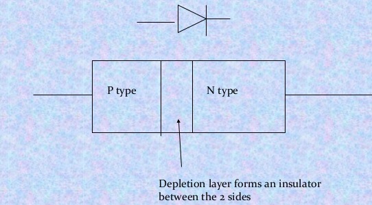
PN Junction Diodes
P type and N type semiconductors, taken separately are of very limited use. If we join a piece of P type material to a piece of N type material such that the crystal structure remains continuous at the boundary a PN JUNCTION is formed that can function as rectifier, amplifier, switching and other operations in electronic circuits.
A PN junction cannot be produced by simply pushing two pieces together or by welding because it gives rise to discontinuities across the crystal structure therefore special fabrication techniques are adopted to form a PN junction.
What is a PN Junction?
A PN junction is a device formed by joining p-type (doped with B, Al) with n-type (doped with P, As, Sb) semiconductors and separated by a thin junction is called PN Junction diode or junction diode.
Electronic Symbol of a PN Junction:
the triangle shows the direction of current In PN junction diode, N is at right and P is at left.
Majority carriers
N region — electrons
P region — holes
Application of PN Junctions:
- Used as rectifiers to convert AC into DC.
- As switch in computer circuits.
- As detectors in radios to detect audio signals
- As LED to emit different colours
Light-emitting diodes LED’s
Light-emitting diodes are designed with a very large band gap so movement of carriers across their depletion region emits Schematic Symbol for a Light Emitting Diode photons of light energy. Lower bandgap LEDs (Light-Emitting Diodes) emit infrared radiation, while LED’s with higher The arrows in the LED bandgap energy emit visible light. representation indicate emitted light. While LED’s emit light, Photo diodes are sensitive to received light. They are constructed so their pn junction can be exposed to the outside through a clear window or lens.
What is a Diode Video Explanation
